Kicad Set Origin
The kicad library convention (klc) is a set of requirements for contributing to the official kicad libraries. Unfortunately, power and ground symbols in kicad are just standard library schematic symbols with the voltage baked into the part itself.
Kicad Move Origin PCB Designs

The purple cross in the center of the footprint shows the component origin and the purple outline shows the component courtyard.

Kicad set origin. I took much of january to play with the kicad nightly builds, tagged kicad 5.99, which will eventually become kicad 6.0.in this article, i document many of the most important changes that the kicad developers have introduced to kicad 6, including numerous. How do i set the dimensions of my pcb in the layout? 2 critical 9 fix committed:
Setting grid origin in footprint library browser causes crash: Allwinner f series (suniv) model: Dimensions for the 0603 package footprint (all values in mm).
Not cheap, but no gain antenna for 80 meters is due to the size of the elements. Users wishing to submit or update library files should be familiar with these guidelines. We do not want you to waste previous hours reading whole chapters only to discover that your recording is unusable due to a preventable technical glitch.
It uses x and y coordinates where the horizontal x coordinate is positive to the right of the origin and negative to the left but the vertical y. I’ve been following the development of kicad for a number of years now, and using it as my main electronics cad package daily for a the last six years or thereabouts, so the release of kicad 6.0. Kicad 6.0 roadmap this document is the kicad version 6 developer's road map document.
Additional third party licenses may also exist in the code base such as the mit license, see the source code for complete and up to date details. One of the a4988 driver does not allow the arduino to turn on, if 32 steps jumper is selected for that specific slot.i.e when m0,m1,m2 is inserted. I am importing odb++ files into a fabrication house software macrofab.
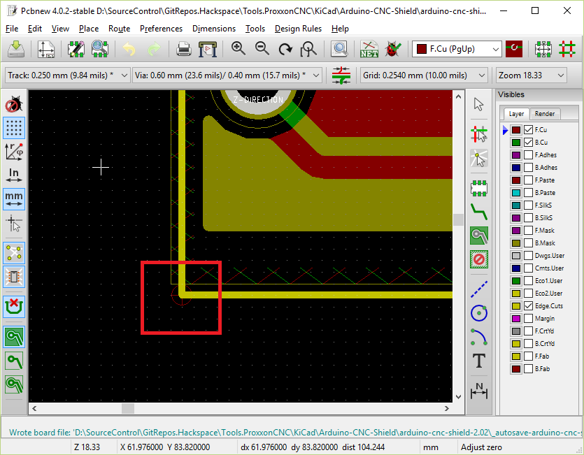
For more information about how.gitignore files work, and how to use them, the following resources are a great place to start: Origin = 0x8020000, length = 384k 第三,在system_stm32f4xx.c文件下修改偏移地址,修改后如下: Place the origin point for drill and place files, set the origin point for the grid。.
Every time the component placement file comes in, it's position is offset from the actual board origin in the gerber files. Origin = 0x20000000, length = 128k flash (rx) : Add reset grid and auxiliary origin commands to menu entry and/or toolbar button.
India on wednesday announced a $10.2 billion plan to try to attract global chipmakers to set up shop in the country and transform it into a production hub of semiconductors. Kicad 6.0 is expected to arrive in the second quarter of 2021 and is the first major release since 2018. All layers related to the top side (top layer, top overlay, top paste, top solder, top dimensions, top component outlines/3d bodies, and top courtyard are all chosen to be.
Allow reset grid and auxiliary origin without hotkey only. My cnc shield is ver3.03 and driver is a4988 set for nema17 for shapeoko2. This is github’s collection of.gitignore file templates.
For a smd pad, set its layer to toplayer or bottomlayer. I set out to verify these assumptions by performing a circuit simulation in kicad. Seth hillbrand 9 fix committed:
59 the official title of iges is digital representation for communication of product definition data, first published in march, 1980 by the u.s. We use this list to populate the.gitignore template choosers available in the github.com interface when creating new repositories and files. Such as kicad, altium designer and others.
Press the space bar at any time to set the new origin. I am using all four driver slots. This is the drill hole diameter for a through hole pad.
Now add a footprint contour. How do i make the component placement files match the pcb 0,0 origin when importing into macrofab software. 2 critical 9 fix committed:
Add support to make all coordinates relative to the plot origin. Click to get the latest buzzing content. When it is set as a slot, the gerber is generated through the stitching of multiple drill holes in the corresponding position.
Finalize feature set and file format. My development system consists of kicad (5.1.2) running on macos mojave. We require new readers to submit a sample recording so that we can make sure that your set up works and that you understand how to export files meeting our technical standards.
I find that when using many altium layers, the default colour scheme can get very confusing. Gcc.git 使用帮助 | 镜像站使用帮助 | 清华大学开源软件镜像站,致力于为国内和校内用户提供高质量的开源软件镜像、linux 镜像源服务,帮助用户更方便地获取开源软件。本镜像站由清华大学 tuna 协会负责运行维护。 Here you can set the pad’s rotation as you want.
Draw an outline of the connector around the component. This means you have to create a new library component if you want to have a rail with a voltage which isn’t in the default set of rail voltage symbols they provide with the installation! The majority of kicad’s source code is developed and distributed under the gnu general public license(gpl) version 3 or greater.
Llvm 使用帮助 | 镜像站使用帮助 | 清华大学开源软件镜像站,致力于为国内和校内用户提供高质量的开源软件镜像、linux 镜像源服务,帮助用户更方便地获取开源软件。本镜像站由清华大学 tuna 协会负责运行维护。 Click on the 'add graphic line or polygon' button in the right toolbar. Kicad crashes when cvpcb or footprint editor opens:
On4un wrote about phased verticals in his classic book, low band dxing, so this isn’t new territory. Package our codes, so that users can install an easyeda in their own os (windows, linux, mac). For symmetrical symbols, the symbol must be centered around the origin (0, 0).
If you are using a different computer setup, the vast majority of this tutorial should still apply, however, some minor changes may be necessary. To make things simple to understand, i like using a ‘hot and cold’ colour scheme. Kicad supports an integrated design workflow in which a schematic and corresponding pcb are designed together, as well as standalone workflows for special uses.
Kicad Set Origin PCB Designs

Kicad Set Origin PCB Designs
Kicad Set Origin Point For Grid Circuit Boards
KiCad 5.0 Grid origin, Drill and place offset and layer alignment targets YouTube

How do I change the orgin? Layout KiCad.info Forums

Kicad Set Origin Point For Grid Circuit Boards
Kicad Set Origin Point For Grid Circuit Boards
Setting origin of coordinates Layout KiCad.info Forums

Kicad Set Origin PCB Designs

Kicad Set Origin Point For Grid Circuit Boards
Kicad Set Origin Point For Grid Circuit Boards
Kicad Set Origin PCB Designs

KiCad 5 footprint editor what are the "Set grid origin" and "place footprint reference anchor

Kicad Set Origin Point For Grid Circuit Boards

How to set grid origin on center of pad in 4.0 RC 1? Layout KiCad.info Forums

How to set grid origin on center of pad in 4.0 RC 1? Layout KiCad.info Forums

Setting origin of coordinates Layout KiCad.info Forums

Origin and it's axis [absolute coordinate origin] Layout KiCad.info Forums

Setting origin of coordinates Layout KiCad.info Forums
